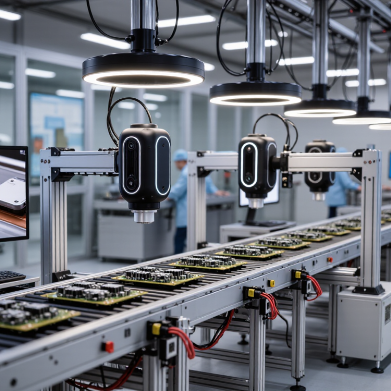
| 2D Machine Vision | Area, shape, color, contrast, position, pattern, and surface appearance | Approximately 10–100 μm per pixel, depending on camera, optics, field of view, and working distance | About 20–500 ms per inspection cycle for a single region of interest; multi-camera systems require additional processing time | Missing components, incorrect orientation, scratches, stains, printing errors, edge damage, label verification, and dimensional deviations in the image plane | High throughput, relatively simple integration, mature lighting techniques, and lower system cost than 3D inspection | Limited ability to measure height, volume, coplanarity, and defects hidden by shadows or overlapping parts | Packaging, connectors, labels, molded parts, textiles, metal surfaces, and electronic assembly verification | Very High |
| 3D Imaging | Height, depth, volume, profile, warpage, flatness, and three-dimensional geometry | Typical height repeatability from approximately 2–50 μm in precision applications; performance varies by sensor and measurement range | Approximately 50–1,000 ms per scan or inspection cycle, depending on scanning method and point-cloud size | Insufficient solder, excessive solder, lifted leads, warpage, missing material, dents, height variation, and surface-profile defects | Provides quantitative height data and detects defects that are difficult to identify with standard 2D imaging | Higher hardware and computing cost; sensitive to reflective, transparent, dark, or highly textured surfaces | PCB assembly, battery cells, automotive components, precision machining, adhesive dispensing, and dimensional inspection | High |
| Automated Optical Inspection (AOI) | Automated visual verification of assembled products using 2D, 3D, or combined imaging | Commonly supports component and solder-feature inspection at approximately 10–50 μm image resolution; exact capability depends on product design | Approximately 3–30 seconds per PCB, depending on board size, component density, camera configuration, and inspection coverage | Wrong or missing components, polarity errors, solder bridges, insufficient solder, lifted leads, tombstoning, bent pins, and assembly defects | Broad defect coverage, traceable inspection records, programmable recipes, and compatibility with inline production lines | False calls can increase with complex reflections, new product variants, poor process control, or insufficient lighting and programming | Surface-mount assembly, through-hole assembly, automotive electronics, industrial controls, and consumer electronics | Very High |
| Solder Paste Inspection (SPI) | Solder-paste area, height, volume, offset, shape, and coverage before component placement | Typical measurement repeatability is commonly within a few micrometers to tens of micrometers, subject to stencil, paste, and equipment conditions | Approximately 3–15 seconds per PCB for inline inspection, depending on board dimensions and measurement density | Insufficient or excessive paste, paste bridging, offset, scooping, clogging, poor release, and missing deposits | Detects printing-process problems early and supports closed-loop control of printing parameters | Cannot verify component placement or final solder-joint quality after reflow; results depend strongly on stencil and paste conditions | SMT production, fine-pitch components, miniature electronics, automotive boards, and high-reliability assemblies | Very High |
| Deep-Learning Vision | Semantic appearance, anomaly patterns, variable shapes, texture, and complex defect classification | Resolution is determined by the camera and optics; model inference commonly operates on image regions from approximately 100 × 100 to several thousand pixels | Approximately 10–200 ms per region of interest on suitable industrial computing hardware; complete cycle time depends on image acquisition and preprocessing | Subtle scratches, cosmetic defects, irregular contamination, texture anomalies, variable assembly conditions, and defects difficult to describe with fixed rules | Handles appearance variation better than rule-based inspection when trained with representative images; reduces manual rule creation for complex patterns | Requires high-quality labeled data, model validation, monitoring for data drift, and careful control of false negatives | Surface inspection, battery materials, fabric, packaging, castings, weld appearance, and complex cosmetic classification | Rapidly Expanding |
| Hybrid 2D + 3D Inspection | Combined appearance, location, height, volume, and geometry analysis | Combines 2D pixel resolution, commonly around 10–100 μm per pixel, with 3D height data that may range from several micrometers to tens of micrometers | Approximately 5–40 seconds per complex PCB or product, depending on the number of views and inspection algorithms | Mixed defects involving both appearance and geometry, such as solder defects with component displacement or surface damage with warpage | More complete defect coverage and improved decision confidence for high-value or high-reliability products | Higher acquisition cost, larger data volume, more demanding calibration, and greater recipe-development effort | Advanced electronics, battery manufacturing, semiconductor packaging, aerospace components, and automotive safety systems | High-Growth |
| Rule-Based Vision with Statistical Process Control | Measured dimensions, defect counts, process trends, and acceptance thresholds | Measurement capability is defined by camera calibration and gauge repeatability; statistical limits are set from historical process data | Typically 20–500 ms for a simple inspection, excluding material handling and communication time | Repeatable dimensional deviations, position errors, missing features, process drift, and threshold-based appearance defects | Transparent decision logic, easy auditability, predictable behavior, and straightforward process monitoring | Less flexible for irregular defects, uncontrolled lighting variation, and products with many legitimate visual variations | Machining, injection molding, packaging, assembly verification, and standardized high-volume production | Very High |